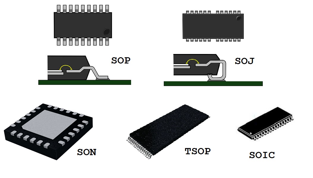
Whether you’re a newbie to PCB design or you’re an experienced professional, you’ll find that there are many different types of PCB package options out there. These include: lead-frame, multichip, and laminated. Choosing the right PCB package type will help ensure that your design will work effectively and efficiently.
Surface mount
Printed Circuit Boards (PCBs) are designed to accommodate several different electronic components. Surface mount pcb packages have been developed to facilitate easier handling during the PCB assembly process.
Surface mount devices are mounted directly onto the PCB without leads. They are typically smaller than through-hole components and have a higher component density. They are also able to provide a higher frequency of operation, which is why they are often used in applications where high frequencies are needed.
The majority of surface mount devices are ICs. They are available in a variety of sizes and packaging types. Some devices require special packages to meet special mechanical, electrical or thermal requirements.
Some of the most common packages are SOPs, QFPs, and QFNs. The small outline transistor (SOT) package is the most widely used. It has a smaller lead count and land pattern than other surface mount components.
Lead-frame
Regardless of the application, there are several different lead-frame pcb package types. The process involves the fabrication of a thin metal sheet, which is then laminated with photo-resist and subsequently etched. The resulting pcb package has various features, including a low thermal resistance and improved electrical properties.
The process can be automated, allowing for high volume production. But it can also be complex and expensive. This is particularly true for high density lead frames. The complexity of the mold tool adds to the cost and increases the possibility of tool failure.
Stamping is a relatively high-speed, automated process that is most suitable for high-volume manufacturing. The die-and-punch sets used to manufacture lead frames are based on the specific geometry of the lead frame. This allows the tool to be time-efficient.
Laminated
During the design process, the type of laminate is important to determine the overall performance of the PCB. It is also essential to choose the right materials. Whether the laminate material is FR4, high temperature or lead free, the choice of the material can have an impact on the overall performance of the board.
The main types of package substrates are flexible, rigid and tape. Each variety has different functional characteristics. It is also important to consider the dielectric constant and the glass transition temperature (Tg) of the laminate.
Besides, there are several other properties that should be taken into consideration. They include fire retardance, moisture absorption and chemical resistance. These properties ensure the safety of the PCB in case of sudden electrical flow. They can be determined by calculating the loss factor, thickness changes with temperature and shear strength.
Multichip
Various IC packages are available in the market. Basically, they can be classified according to their mounting style and the substrate technology. Some of the common types of IC packages are DIP, SOP, QSOP, SSP, BGA, TQFP, and SSOP.
A DIP package is a plastic dual-in-line package with two parallel rows of electrical connecting pins. DIPs can be mounted directly on the PCB, but they can also be inserted into a socket or a socket connector. DIPs are used for prototyping boards, since the pins are spaced at 0.1 inches (2.54mm) apart.
A SOP package is similar to a DIP, except that it has four lead directions instead of two. A Quad Flat L-leaded Package is similar to a SOP, except that it has a built-in heat spreader. A Thin Small Outline Package is a rectangular IC component with tiny pins on the horizontal edges. This type is often used for ICs that power RAMs or flash memory.
Area array
Several PCB package types exist, each of which has its own characteristics. There are two major types of arrays: ball grid arrays (BGAs) and land grid arrays (LGAs). Each has its advantages and disadvantages.
Regardless of the type of PCB you use, you will need to have a substrate. The substrate is typically made of a polyimide material, although ceramic versions are available. For high reliability applications, ceramic packages are preferred. MBGAs, which are metal ceramic, are particularly good for thermal heat dissipation values. They also have excellent electrical performance.
Unlike traditional circuit boards, the interconnection process is based on an array of solder balls. These are 0.5-0.7mm in diameter and are made from a tin-lead eutectic alloy. They are attached to a copper line through microwelding or solder reflow. This allows for precise jetting of molten solder on the component.


